- 您现在的位置:买卖IC网 > Sheet目录1245 > SPI-324P-O4-N1 (Lattice Semiconductor Corporation)IP PHY LAYER BRIDGE SPI3-4 ORCA4
�� �
�
�Quad� SPI-3� to� SPI-4� Link� Layer�
�Lattice� Semiconductor�
�Bridge� Core� User’s� Guide�
�Receive� Logical� Timing�
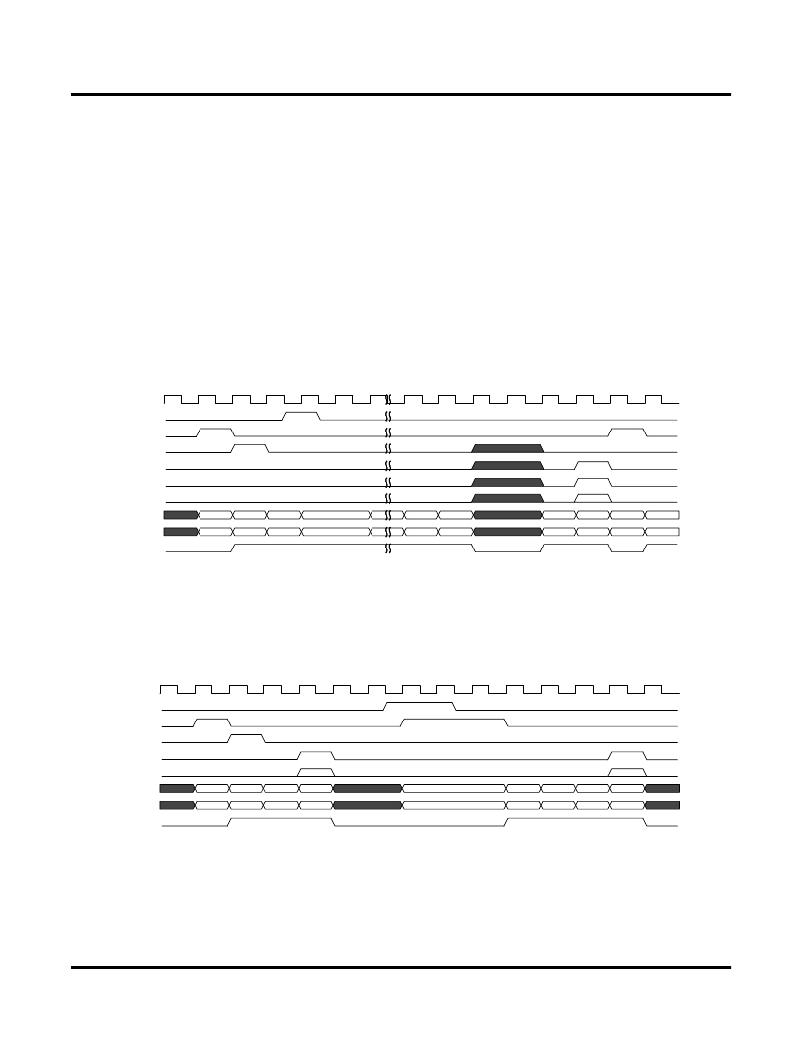
�Figure� 6� shows� transactions� on� a� SPI-3� Receive� interface� with� two� ports.� The� SPI-3� Receive� Interface� is� controlled�
�by� the� Link� Layer� device� using� the� RENB� signal.� All� signals� must� be� updated� and� sampled� using� the� rising� edge� of�
�the� receive� FIFO� clock.� The� RDAT� bus,� RPRTY,� RMOD,� RSOP,� REOP� and� RERR� signals� are� valid� in� cycles� for�
�which� RVAL� is� high� and� RENB� was� low� in� the� previous� cycle.� When� transferring� data,� RVAL� is� asserted� and�
�remains� high� until� the� internal� FIFO� of� the� PHY� Layer� device� is� empty� or� an� end� of� packet� is� transferred.� The� RSX�
�signal� is� valid� in� the� cycle� for� which� RVAL� is� low� and� RENB� was� low� in� the� previous� cycle.�
�The� PHY� informs� the� Link� Layer� device� of� the� port� address� of� the� selected� FIFO� by� asserting� RSX� with� the� port�
�address� on� the� RDAT� bus.� The� Link� Layer� may� pause� the� Receive� Interface� at� any� time� by� de-asserting� the� RENB�
�signal.� When� the� selected� FIFO� is� empty,� RVAL� is� de-asserted.� In� this� example,� the� RVAL� is� re-asserted,� without�
�changing� the� selected� FIFO,� transferring� the� last� section� of� the� packet.� The� end� of� the� packet� is� indicated� with� the�
�REOP� signal.� Thus,� the� next� subsequent� FIFO� transfer� for� this� port� would� be� the� start� of� the� next� packet.� If� an� error�
�occurred� during� the� reception� of� the� packet,� the� RERR� would� be� asserted� with� REOP.� Since� another� port’s� FIFO�
�has� suf?cient� data� to� initiate� a� bus� transfer,� RSX� is� again� asserted� with� the� port� address.� In� this� case,� an� intermedi-�
�ate� section� of� the� packet� is� being� transferred.�
�Figure� 6.� Transactions� on� the� SPI-3� Receive� Interface�
�RFCLK�
�RENB�
�RSX�
�RSOP�
�REOP�
�RERR�
�RMOD[1:0]�
�RDAT[31:0]�
�0000�
�B1-B4�
�B5-B8�
�B9-B12�
�B41-B44� B45-B48�
�B52-B55� B56-B57�
�0001�
�B21-B25�
�RPRTY�
�RVAL�
�Figure� 7� shows� the� use� of� the� pause� feature� of� the� receive� interface.� The� ?rst� transfer� is� a� complete� 3-byte� packet�
�and� the� second� transfer� is� the� end� of� a� 36-byte� packet.� The� pause� allows� the� Link� Layer� device� to� halt� data� between�
�transfers.� In� order� to� handle� an� end� of� packet,� the� Link� Layer� device� may� de-assert� the� RENB� signal� when� it� sam-�
�ples� REOP� active.� As� shown� in� the� diagram,� the� Link� Layer� device� pauses� the� PHY� device� on� the� in-band� address�
�for� two� clock� cycles.�
�Figure� 7.� Receive� Interface� Transactions� with� Pausing�
�RFCLK�
�RENB�
�RSX�
�RSOP�
�REOP�
�RERR�
�RDAT[7:0]�
�03�
�B1�
�B2�
�B3�
�01�
�B33�
�B34�
�B35�
�B36�
�RPRTY�
�RVAL�
�15�
�发布紧急采购,3分钟左右您将得到回复。
相关PDF资料
SPN02SVBN-RC
CONN JUMPER SHORTING 2MM GOLD
SPN02SVEN-RC
CONN JUMPER SHORTING 2MM GOLD
SPN02SXCN-RC
CONN JUMPER SHORTING 2MM GOLD
SPT711XPFCE
CARD TELEPHONY FARM CRD 711X
SPUSB1AJT
SURGE SUPPRESOR USB 12OHM SC70-6
SR-5H-6.3A-BK
FUSE 6.3A 250VAC RADIAL SLOW
SR1K20M155X
VARISTOR 20VRMS W/RFI SUPP RAD
SRP120LF
POLYSWITCH PTC RESET 1.2A STRAP
相关代理商/技术参数
SPI-333-34AB
制造商:SANYO Semiconductor Co Ltd 功能描述:
SPI-335-34
制造商:SANYO 制造商全称:Sanyo Semicon Device 功能描述:Ultraminiature photoreflector (single-transistor type)
SPI-336-99-T1
制造商:SANYO 制造商全称:Sanyo Semicon Device 功能描述:Ultraminiature photoreflector supporting reflow soldering Single transistor type
SPI3501UH
制造商:SPI 制造商全称:SPI 功能描述:350 Watts EPS12V 1U Switching Power Supply
SPI3501UH-B204
制造商:Sparkle Power Inc 功能描述:POWER SUPPLY,SWITCHING,ENCLOSED,1U,350 WATT,ATX/EPS,PFC,(2)1
SPI350ACA8
制造商:SPI 制造商全称:SPI 功能描述:350 Watts, ATX Switching Power Supply
SPI350ACAG
制造商:SPI 制造商全称:SPI 功能描述:350 Watts ATX12V 2.3 Switching Power Supply Meet 2010 ErP
SPI350GLN
制造商:Sparkle Power Inc 功能描述:POWER SUPPLY,SWITCHING,ATX,350 WATT,ATX12V 2.2,PFC,(2)12VDC@